BGA Chips Reball Automatic Optic Align
BGA Chips Reball Automatic Optic Align. Suitable for different SMD SMT components.
Description
BGA Chips Reball Automatic Optic Align
BGA (Ball Grid Array) chips are a type of integrated circuit package that is popular in modern electronic devices.
Reballing is a process where the solder balls on the underside of the BGA chip are removed and replaced with new ones. This may be necessary if the original solder balls become damaged, or if the chip needs to be reworked for some other reason.


1.Application Of laser positioning BGA Chips Reball Automatic Optic Align
Work with all kinds of motherboards or PCBA.
Solder, reball, desoldering different kind of chips: BGA,PGA,POP,BQFP,QFN,SOT223,PLCC,TQFP,TDFN,TSOP, PBGA,CPGA,LED chip.
DH-G620 is totally same as DH-A2, automatically desoldering, pick-up, puting back and soldering for a chip, with optical alignment for mounting,no matter whether you have experience or not, you can master it in one hour.

2.Product Features of BGA Chips Reball Automatic Optic Align

3.Specification of DH-A2 BGA Chips Reball Automatic Optic Align
| power | 5300W |
| Top heater | Hot air 1200W |
| Bottom heater | Hot air 1200W.Infrared 2700W |
| Power supply | AC220V±10% 50/60Hz |
| Dimension | L530*W670*H790 mm |
| Positioning | V-groove PCB support, and with external universal fixture |
| Temperature control | K type thermocouple, closed loop control, independent heating |
| Temperature accuracy | ±2℃ |
| PCB size | Max 450*490 mm,Min 22*22 mm |
| Workbench fine-tuning | ±15mm forward/backward,±15mm right/left |
| BGAchip | 80*80-1*1mm |
| Minimum chip spacing | 0.15mm |
| Temp Sensor | 1(optional) |
| Net weight | 70kg |
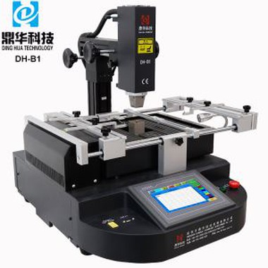
4. Details of BGA Chips Reball Automatic Optic Align
Automatic optic alignment is a feature of some reballing machines that allows for precise alignment of the BGA
chip during the reballing process. The machine uses a camera and advanced image recognition algorithms to align
the chip perfectly over the center of the target area, thus ensuring that the new solder balls will be applied in the
correct position.

Overall, the combination of BGA chip reballing and automatic optic alignment technology is a powerful tool for
repairing and maintaining electronic devices, and can help to extend their lifespan and reduce costs associated
with replacement.


5.Why Choose Our BGA Chips Reball Automatic Optic Align Split Vision?


6.Certificate of BGA Chips Reball Automatic Optic Align
UL, E-MARK, CCC, FCC, CE ROHS certificates. Meanwhile, to improve and perfect the quality system, Dinghua has passed ISO, GMP, FCCA, C-TPAT on-site audit certification.

8.Shipment for BGA Chips Reball Automatic Optic Align
DHL/TNT/FEDEX. If you want other shipping term, please tell us. We will support you.
9. Terms of Payment
Bank transfer, Western Union, Credit Card.
Please tell us if you need other support.
11. Related Knowledge
Why is the connection between the ground and the casing of the PCB (connected to earth) necessary? Is it possible to use only capacitors?
The existing answer is not accurate, so let me explain.
1,Capacitor Connection: From the perspective of EMS (Electromagnetic Immunity), this capacitor relies on the premise that PE (Protective Earth) is well connected to the ground. This connection can reduce the high-frequency interference in the circuit by providing a reference to ground level. The effect is to suppress transient common-mode differentials between the circuit and the interferer. Ideally, GND should be directly connected to PE, but this may not always be feasible or safe. For example, the GND generated after rectifying 220V AC cannot be connected to PE, which affects the low-frequency path and allows high-frequency signals to pass. From the perspective of EMI (electromagnetic interference), having a metal casing connected to PE can also help avoid high-frequency signal radiation.
2,1M Resistor Use: The 1M resistor is important for ESD (electrostatic discharge) testing. Because this system connects PE and GND through a capacitor (floating system), during ESD testing, the charge driven into the circuit under test is released gradually, raising or lowering the level of GND relative to PE. If the accumulated voltage exceeds the tolerable range for the weakest insulation between PE and the circuit, it will discharge between GND and PE, generating tens to hundreds of amps on the PCB within a few nanoseconds. This current is sufficient to damage any circuit due to EMP (electromagnetic pulse) or through a device connecting PE to the signal at the weakest insulation point. However, as mentioned earlier, sometimes I cannot directly connect PE and GND. In such cases, I use a 1-2M resistor to slowly release the charge and eliminate the voltage difference between the two. The value of 1-2M is chosen based on the ESD test standard; for instance, the highest repetition rate specified in IEC61000 is only 10 times per second. If non-standard ESD discharge occurs at 1000 times per second, then a 1-2M resistance may not be sufficient to release the accumulated charge.
3,Capacitance Value: The capacitance value suggested by the subject is too large; typically, a value of about 1nF is suitable. If a significantly larger capacitance is used in industrial equipment such as inverters and servo drivers with switching frequencies of 8-16 kHz, there is a risk of electric shock when users touch the outer casing. A large capacitance may indicate deficiencies in other circuit designs, necessitating an increase in this capacitance to address EMC testing.
Finally, let me emphasize: PE is not reliable! Many domestic customers may not provide a valid PE connection, meaning you cannot depend on PE to improve EMS or reduce EMI. This situation is not entirely the customers' fault; their workshops, factories, and offices often do not adhere to electrical standards, lacking proper grounding. Therefore, understanding the unreliability of PE, I employ various techniques to enhance the circuit's resistance to EMS testing.