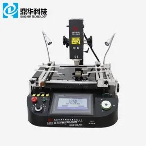
DHA2 BGA Rework Station
DHA2 BGA Rework Station with split vision for automatic mouninting, also automatically soldering, picking up and soldering for various chips.
Description
Automatic DHA2 BGA Rework Station
An automatic DHA2 BGA rework station is equipment used for repairing and replacing ball grid array (BGA) components on printed circuit boards (PCBs). These rework stations utilize advanced technology, such as infrared heating, hot air convection, and computer-controlled precision, to remove and replace BGAs without damaging surrounding components.
The DHA2 BGA rework station typically includes features like a built-in temperature profiling system, adjustable airflow control, and real-time temperature monitoring. These features ensure the BGA is heated and cooled at a controlled rate, reducing the risk of thermal damage to nearby components. Additionally, computer-controlled precision enables repeatable and reliable results, making the rework process efficient and consistent.
In summary, an automatic DHA2 BGA rework station is a valuable tool for electronics repair and maintenance, providing a quick and effective way to replace faulty BGAs with minimal risk to surrounding components.


1.Application Of laser positioning DHA2 BGA Rework Station
Work with all kinds of motherboards or PCBA.
Solder, reball, desoldering different kind of chips: BGA,PGA,POP,BQFP,QFN,SOT223,PLCC,TQFP,TDFN,TSOP,
PBGA,CPGA,LED chip.
DH-G620 is totally same as DH-A2, automatically desoldering, pick-up, puting back and soldering for a chip, with optical alignment for mounting,no matter whether you have experience or not, you can master it in one hour.

2.Specification of DHA2 BGA Rework Station
| power | 5300W |
| Top heater | Hot air 1200W |
| Bottom heater | Hot air 1200W.Infrared 2700W |
| Power supply | AC220V±10% 50/60Hz |
| Dimension | L530*W670*H790 mm |
| Positioning | V-groove PCB support, and with external universal fixture |
| Temperature control | K type thermocouple, closed loop control, independent heating |
| Temperature accuracy | ±2℃ |
| PCB size | Max 450*490 mm,Min 22*22 mm |
| Workbench fine-tuning | ±15mm forward/backward,±15mm right/left |
| BGAchip | 80*80-1*1mm |
| Minimum chip spacing | 0.15mm |
| Temp Sensor | 1(optional) |
| Net weight | 70kg |
3.Details of Laser Positioning DHA2 BGA Rework Station


4.Certificate of Automatic DHA2 BGA Rework Station
UL, E-MARK, CCC, FCC, CE ROHS certificates. Meanwhile, to improve and perfect the quality system,
Dinghua has passed ISO, GMP, FCCA, C-TPAT on-site audit certification.

5.Packing & Shipment of DHA2 BGA Rework Station with CCD Camera

6.Shipment for Laser DHA2 BGA Rework Station with Optical alignment
DHL/TNT/FEDEX. If you want other shipping term, please tell us. We will support you.
7. Terms of Payment
Bank transfer, Western Union, Credit Card.
Please tell us if you need other support.
8. Related Knowledge
Detailed Explanation of the Reverse Principle of PCB Copy Boards
The reverse principle of PCB copy boards involves analyzing the principles and operating conditions of a circuit board based on a reverse schematic, allowing for an understanding of the product's functional characteristics. This reverse schematic may involve reproducing the PCB layout from files or directly drawing the circuit diagram from a physical product. In standard forward design, product development generally starts with schematic design, followed by PCB layout based on that schematic.
Whether used to analyze board principles and product characteristics in reverse engineering, or as a reference for forward PCB design, schematics serve a unique purpose. So, when working with the document or a physical product, what details should be noted to reverse-engineer the PCB schematic effectively?
1. Reasonable Division of Functional Areas
When reverse-engineering the schematic of a PCB, dividing functional areas can help engineers avoid unnecessary complications and improve the efficiency of drawing. Typically, components with similar functions on a PCB are grouped together, making functional division a useful basis when reconstructing the schematic.
However, this division of functional areas requires a solid understanding of electronic circuit principles. Start by identifying the core components in a functional unit, then trace connections to locate other components within the same unit. Functional partitions form the basis for schematic drawing. Don't forget to reference component serial numbers, as they can expedite functional area division.
2. Correctly Identifying and Drawing Connections
For identifying ground, power, and signal lines, engineers need to understand power circuits, connection principles, and PCB routing. These distinctions can often be deduced from component connections, circuit copper width, and product characteristics.
When drawing, to avoid line crossings and interferences, grounding symbols can be used generously. Different colors can be applied to distinguish various lines, and special symbols can mark specific components. Individual unit circuits may also be drawn separately and later combined.
3. Selecting a Reference Component
This reference component serves as the main anchor when beginning a schematic drawing. Determining the reference component first, then drawing based on its pins, ensures greater accuracy in the final schematic.
Choosing the reference component is generally straightforward. Main circuit components, often large with multiple pins, are suitable as reference points. Integrated circuits, transformers, and transistors are typical examples of useful reference components.
4. Using a Basic Framework and Similar Schematics
Engineers should master the basic layout of common circuits and schematic drawing techniques. This knowledge helps in constructing simple and classic unit circuits and forming the broader framework of electronic circuits.
It is also helpful to refer to schematics of similar electronic products, as similar products often share circuit design elements. Engineers can utilize experience and existing diagrams to assist in the reverse engineering of new product schematics.
5. Verification and Optimization
Once the schematic drawing is complete, it's essential to conduct tests and cross-checks to finalize the reverse-engineering process. The nominal values of components sensitive to PCB distribution parameters should be reviewed and optimized. Comparing the reverse-engineered schematic with the PCB file diagram ensures consistency and accuracy across both diagrams.