BGA Rework Station SP360c PS3 PS4
1. Effective repairing motherboards of PS3,PS4,SP360C,mobile, laptop. 2. Cross-flow cooling fan ensure automatic cooling function, which ensure long lifespan and avoid damage. 3. Infrared laser positioning helps position motherboard easily and fast. 4. High definition Touch screen.
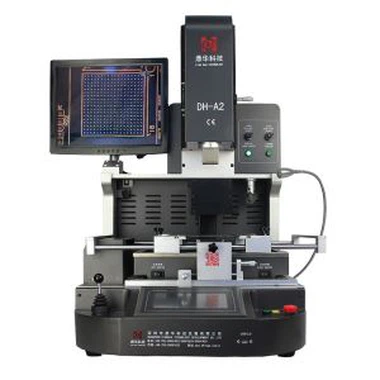
Description
1.Application Of Automatic BGA Rework Station for SP360c PS3 PS4
Work with all kinds of motherboards or PCBA.
Solder, reball, desoldering different kind of chips: BGA,PGA,POP,BQFP,QFN,SOT223,PLCC,TQFP,TDFN,TSOP, PBGA,CPGA,LED chip.

2.Product Features of Automatic BGA Rework Station for SP360c PS3 PS4

3.Specification of Automatic BGA Rework Station for SP360c PS3 PS4
| Power | 5300W |
| Top heater | Hot air 1200W |
| Bollom heater | Hot air 1200W, Infrared 2700W |
| Power supply | AC220V± 10% 50/60Hz |
| Dimension | L530*W670*H790 mm |
| Posilioning | V-groove PCB support, and with external universal fixture |
| Temperature control | K type thermocouple. closed loop control. independent heating |
| Temperalure accuracy | ±2℃ |
| PCB size | Max 450*490 mm, Min 22*22 mm |
| Workbench fine-tuning | ±15mm forward/backward, ±15mm righ/left |
| BGAchip | 80*80-1*1mm |
| Minimum chip spacing | 0.15mm |
| Temp Sensor | 1(opional) |
| Net weight | 70kg |
4.Details of Automatic BGA Rework Station for SP360c PS3 PS4


5.Why Choose Our Automatic BGA Rework Station for SP360c PS3 PS4?


6.Certificate of Automatic BGA Rework Station for SP360c PS3 PS4
UL, E-MARK, CCC, FCC, CE ROHS certificates. Meanwhile, to improve and perfect the quality system, Dinghua has passed ISO, GMP, FCCA, C-TPAT on-site audit certification.

7.Packing & Shipment of Automatic BGA Rework Station for SP360c PS3 PS4

8.Shipment for Automatic BGA Rework Station for SP360c PS3 PS4
DHL/TNT/FEDEX. If you want other shipping term, please tell us. We will support you.
9. Terms of Payment
Bank transfer, Western Union, Credit Card.
Please tell us if you need other support.
11. Related Knowledge
Bubble Treatment During Rework
In assemblies with bottom termination components (BTC), the presence of air bubbles has been a serious problem for many applications. To define bubbles, the following is a description of soldering defects:
[...] Tin melts quickly to fill the appropriate gaps and captures some flux in the solder joints. These trapped flux bubbles are hollow; [...] These voids prevent the tin from filling the joint completely. In such solder joints, the solder cannot fill the entire joint because the flux has been sealed inside. [1]
In the SMT field, bubbles can lead to the following effects: [...] Since there is a limited amount of solder that can be applied to each joint, the reliability of the solder joints is a primary concern. The presence of bubbles has been a common drawback associated with solder joints, especially during reflow soldering in SMT. Bubbles can weaken the solder joint's strength, ultimately leading to solder joint failure. [2]
The impact on solder joint quality due to bubble formation has been discussed many times in various forums:
- Reduced heat transfer from the component to the PCB, increasing the risk of excessive component body temperature.
- Reduced mechanical strength of the solder joints.
- Gas escaping from the solder joint, potentially causing solder splashes.
- Reduced current-carrying capacity of the solder joint (amperage capacity) – the junction temperature rises due to increased resistance in the solder joint.
- Signal transmission issues – in high-frequency applications, bubbles can weaken the signal.
This issue is especially prominent in power electronics, where bubble formation on thermal pads (such as QFN package components) is becoming an increasing concern. Heat must be transferred from the component to the PCB for dissipation. When this critical process is compromised, the component's lifespan is significantly shortened.
Conventional Methods for Reducing Bubbles:
Some conventional methods for reducing bubbles include using low-bubble solder paste, optimizing the reflow profile, and adjusting the stencil openings to apply the optimal amount of solder paste. Additionally, addressing bubble formation when the solder paste is in its liquid state is another important aspect of the solution throughout the electronic assembly process.
So, the question arises: how can the bubble treatment process be applied in an open environment like rework equipment? The vacuum technology used in reflow soldering is clearly not suitable. A technique based on sinusoidal excitation of the PCB substrate is more appropriate for rework (Figure 1). First, the PCB is excited by a longitudinal wave with an amplitude of less than 10 μm. This sine wave excites the PCB at a specific frequency. In this region, both the PCB body and the solder joints on the PCB resonate under stress. When the PCB is exposed to energy, the components remain in place, and the bubbles are forced into the edge regions of the liquid solder, allowing them to escape from the solder joints.
By using this method, the bubble ratio can be reduced to 2% in the soldering of new components (Fig. 2). Even with this technique, significant bubble removal can be achieved on the target solder joints on the assembled PCB during the secondary reflow process. In this re-bubbling rework process, only the selected area on the PCB is heated to reflow temperatures, and only this area is sinusoidally excited, so there is no negative impact on the entire product.
Scanning Waves are longitudinally propagated along the PCB substrate.
The excitation is performed by a linear scanning wave produced by a piezoelectric actuator.
- Handling bubbles in PCBA with a piezo driver.
- Activating the excitation function during reflow to significantly reduce the proportion of bubbles in the MLF (before and after application).