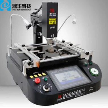
Hot Air SMD Rework Station
Hot air SMD rework stations are commonly used in electronics repair, PCB prototyping, and product assembly. They are favored over other rework methods, such as soldering irons, due to their precision, speed, and ability to remove and replace components without damaging the surrounding components or PCB
Description
Automatic Hot Air SMD Rework Station
A Hot Air SMD Rework Station is a device used in electronics repair and assembly. It is specifically designed for removing and replacing Surface Mount Devices (SMDs) on printed circuit boards (PCBs). The hot air rework station operates by directing a stream of hot air over the SMD, heating the solder joints until they melt, which allows the component to be lifted off the board. The hot air is generated by a heating element controlled by a temperature controller. Once the SMD has been removed, the new component can be placed on the board and soldered using the same hot air process.

1.Application Of laser positioning Hot Air SMD Rework Station
Work with all kinds of motherboards or PCBA.
Solder, reball, desoldering different kind of chips: BGA,PGA,POP,BQFP,QFN,SOT223,PLCC,TQFP,TDFN,TSOP,
PBGA,CPGA,LED chip.
DH-G620 is totally same as DH-A2, automatically desoldering, pick-up, puting back and soldering for a chip, with optical alignment for mounting,no matter whether you have experience or not, you can master it in one hour.

2.Product Features of Optical Alignment

3.Specification of DH-A2
| power | 5300W |
| Top heater | Hot air 1200W |
| Bottom heater | Hot air 1200W.Infrared 2700W |
| Power supply | AC220V±10% 50/60Hz |
| Dimension | L530*W670*H790 mm |
| Positioning | V-groove PCB support, and with external universal fixture |
| Temperature control | K type thermocouple, closed loop control, independent heating |
| Temperature accuracy | ±2℃ |
| PCB size | Max 450*490 mm,Min 22*22 mm |
| Workbench fine-tuning | ±15mm forward/backward,±15mm right/left |
| BGAchip | 80*80-1*1mm |
| Minimum chip spacing | 0.15mm |
| Temp Sensor | 1(optional) |
| Net weight | 70kg |
4.Why Choose Our Hot Air SMD Rework Station Split Vision?

5.Certificate of Hot Air SMD Rework Station Optic Align
UL, E-MARK, CCC, FCC, CE ROHS certificates. Meanwhile, to improve and perfect the quality system,
Dinghua has passed ISO, GMP, FCCA, C-TPAT on-site audit certification.

6.Packing & Shipment of Hot Air SMD Rework Station

7.Shipment for Hot Air SMD Rework Station
DHL/TNT/FEDEX. If you want other shipping term, please tell us. We will support you.
8. Terms of Payment
Bank transfer, Western Union, Credit Card.
Please tell us if you need other support.
9. Related knowledge
With the rapid development of mobile phones, computers, and the electronic digital industries, the PCB circuit board industry is constantly adapting to meet the needs of the market and consumers, which has driven the continuous increase in the industry's output value. However, competition in the PCB circuit board industry is intensifying, and many PCB manufacturers are willing to spare no expense. They lower prices and exaggerate production capacity to attract a large number of customers. However, low-priced PCB boards must use cheap materials, which affects product quality, shortens service life, and makes the products prone to surface damage, bumps, and other quality problems.
The purpose of PCB circuit board proofing is to assess the manufacturer's capabilities, which can effectively reduce the non-performance rate of PCB circuit boards and lay a solid foundation for future mass production.
PCB Circuit Board Proofing Process:
First, Contact the Manufacturer:
First, we need to provide the manufacturer with the necessary documents, process requirements, and quantity. What parameters do you need to provide for the PCB circuit board proofing? You can click here to get the information you need. Then, professionals will quote you, place the order, and follow up on the production schedule.
Second, Material:
Purpose: Cut the large sheet material into small pieces that meet the requirements according to the engineering data MI, ensuring that the small sheets meet the customer's specifications.
Process: Large sheet material → cut into smaller boards according to MI requirements → board → beer fillet/edging → exit board.
Third, Drilling:
Purpose: Drill the required hole diameter at the corresponding positions on the sheet of the required size based on the engineering data.
Process: Stacking pin → upper plate → drilling → lower plate → inspection/repair.
Fourth, Sink Copper:
Purpose: Deposit copper by chemically applying a thin layer of copper on the walls of the insulating holes.
Process: Coarse grinding → hanging board → copper-plated automatic line → lower board → dip in 1% diluted H2SO4 → thick copper.
Fifth, Graphics Transfer:
Purpose: Transfer images from the production film to the board.
Process: (Blue oil process): grinding board → printing the first side → drying → printing the second side → drying → exposure → shadowing → inspection; (dry film process): hemp board → laminating → standing → right bit → exposure → rest → shadow → check.
Sixth, Graphic Plating:
Purpose: Perform graphic plating on the bare copper of the line pattern, or electroplate a layer of copper to the required thickness, along with a layer of gold, nickel, or tin to the required thickness on the walls of the holes.
Process: Upper plate → degreasing → water washing twice → micro-etching → water washing → pickling → copper plating → water washing → pickling → tin plating → water washing → lower plate.
Seventh, Unwinding:
1,Purpose: Remove the anti-plating coating layer with NaOH solution to expose the non-line copper layer.
2,Process: Water film: inserting → soaking in alkali → washing → scrubbing → passing machine; dry film: placing board → passing machine.
Eighth, Etching:
Purpose: Use chemical reactions to corrode the copper layer in non-line parts.
Ninth, Green Oil:
Purpose: Transfer the pattern of the green oil film to the board to protect the line and prevent solder from flowing onto the line when attaching components.
Process: Grinding plate → printing photosensitive green oil → curing plate → exposure → shadowing; grinding plate → printing the first side → baking sheet → printing the second side → baking sheet.
Tenth, Characters:
Purpose: Characters serve as easily recognizable marks.
Process: After curing the green oil → cooling down → adjusting the network → printing characters.
Eleventh, Gold-Plated Fingers:
Purpose: Plate a layer of nickel/gold to the required thickness on the plug finger to enhance rigidity and wear resistance.
Process: Upper plate → degreasing → water washing twice → micro-etching → water washing twice → pickling → copper plating → water washing → nickel plating → water washing → gold plating.
Tin Plate (a juxtaposition process):
Purpose: Spray tin onto the bare copper surface not covered with solder resist oil to protect it from oxidation and ensure good soldering performance.
Process: Micro-etching → air drying → preheating → rosin coating → solder coating → hot air leveling → air cooling → washing and drying.
Twelfth, Molding:
Purpose: Use die stamping or CNC machining to cut out the required shape for customers, including organic enamel, beer board, and hand-cut options.
Note: The accuracy of the data board and the beer board is higher, while hand-cutting is less precise. The hand-cut board can only create simple shapes.
Thirteenth, Testing:
Purpose: Perform electronic 100% testing to detect open circuits, short circuits, and other defects that are not easily found by visual observation.
Process: Upper mold → release board → test → qualified → FQC visual inspection → unqualified → repair → retest → OK → REJ → scrap.
Fourteenth, Final Inspection:
Purpose: Conduct a 100% visual inspection for appearance defects and repair minor defects to prevent defective boards from being released.
Specific Workflow: Incoming materials → view data → visual inspection → qualified → FQA random inspection → qualified → packaging → unqualified → processing → check OK!
Due to the high technical requirements in the design, processing, and manufacturing of PCB circuit boards, only by maintaining precision and strict adherence to every detail in PCB proofing and production can high-quality PCB products be achieved, thereby winning the favor of more customers and gaining a larger market share.