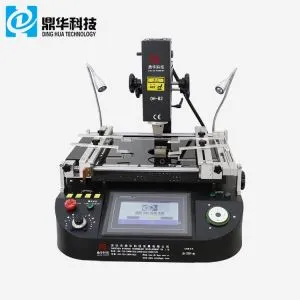
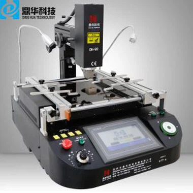
BGA Repair Machine Reballing Motherboard
1.BGA Repair Machine Reballing Motherboard. 2.DH-A2 3.Heating: hot air and infrared. 4.Optic alignment.
Description
BGA Repair Machine for Reballing Motherboard


1.Application Of laser positioning BGA Repair Machine for Reballing Motherboard
Work with all kinds of motherboards or PCBA.
Solder, reball, desoldering different kind of chips: BGA,PGA,POP,BQFP,QFN,SOT223,PLCC,TQFP,TDFN,TSOP, PBGA,CPGA,LED chip.
2.Product Features of Optical Alignment BGA Repair Machine for Reballing Motherboard

3.Specification of DH-A2 BGA Repair Machine for Reballing Motherboard

4.Details of Hot Air BGA Repair Machine for Reballing Motherboard


5.Why Choose Our Infrared BGA Repair Machine for Reballing Motherboard Split Vision?


6.Certificate of CCD Camera BGA Repair Machine for Reballing Motherboard
UL, E-MARK, CCC, FCC, CE ROHS certificates. Meanwhile, to improve and perfect the quality system, Dinghua has passed ISO, GMP, FCCA, C-TPAT on-site audit certification.

7.Packing & Shipment of Automatic BGA Repair Machine for Reballing Motherboard

8.Shipment for BGA Repair Machine for Reballing Motherboard
DHL/TNT/FEDEX. If you want other shipping term, please tell us. We will support you.
9. Terms of Payment
Bank transfer, Western Union, Credit Card.
Please tell us if you need other support.
10. How DH-A2 IBGA Repair Machine work?
11. Related knowledge
PCB circuit board classification
According to the number of circuit layers: divided into single-panel, double-panel and multi-layer boards. Common multi-layer boards are generally 4-layer boards or 6-layer boards, and complex multi-layer boards can reach dozens of layers.
Single-Sided Boards On the most basic PCB boards, the parts are concentrated on one side, and the wires are concentrated on the other side (when the chip components are on the same side as the wires, the plug-in devices are on the other side). Since the wire is only present on one side, the PCB board is called a single-sided. Because single-panel has many strict restrictions on the design line (because there is only one side, the wiring can not cross and must be around the path), so only the early circuit used this type of board.
Double-Sided Boards This type of PCB has wiring on both sides, but to use the two sides of the wire, you must have proper circuit connections between the two sides. The "bridge" between such circuits is called a via. The via hole is a small hole filled or coated with metal on the PCB, which can be connected to the wires on both sides. Because the area of the double panel is twice as large as that of the single panel, the double panel solves the difficulty of wiring interleaving in a single panel (which can be conducted through the hole to the other side), which is more suitable for circuits that are more complicated than single panels.
Multi-Layer Boards In order to increase the area that can be routed, multi-layer boards use more single or double-sided wiring boards. Using a double-sided inner layer, two single-sided outer layers or two double-sided inner layers, two single-sided outer printed circuit boards, alternating between the positioning system and the insulating bonding material and conductive patterns Printed circuit boards that are interconnected according to design requirements become four-layer, six-layer printed circuit boards, also known as multilayer printed wiring boards. The number of layers in the board does not mean that there are several separate wiring layers. In special cases, empty layers are added to control the thickness of the board. Usually the number of layers is even and the outermost two layers are included. Most of the motherboards are 4 to 8 layers of structure, but technically they can achieve nearly 100 layers of PCB. Large supercomputers mostly use quite a few multi-layer motherboards, but because such computers can already be replaced by clusters of many common computers, super-multilayer boards have gradually disappeared. Because the layers in the PCB are tightly bonded, it is not easy to see the actual number, but if you look closely at the motherboard, you can still see it.