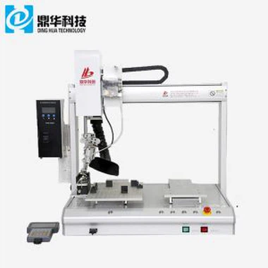
Station Reballing BGA Tech
1. Latest tech in BGA reballing station field.
2. Latest technologies are adopted in heating system and optical alignment system.
3. Available in stock! Welcome to order.
4. Can reball different chips of different motherboards.
Description
Station Reballing BGA Tech
Station reballing BGA tech refers to the process of replacing the solder balls on a Ball Grid Array (BGA) chip.
BGA is a type of surface-mount packaging used for integrated circuits, where the chip is mounted on a PCB
using an array of small balls of solder.


1.Application Of Automatic Station Reballing BGA Tech
Work with all kinds of motherboards or PCBA.
Solder, reball, desoldering different kind of chips: BGA,PGA,POP,BQFP,QFN,SOT223,PLCC,TQFP,TDFN,TSOP,
PBGA,CPGA,LED chip.
2.Product Features of Automatic Station Reballing BGA Tech

3.Specification of Automatic Station Reballing BGA Tech

4.Details of Automatic Station Reballing BGA Tech


5.Why Choose Our Automatic Station Reballing BGA Tech?


6.Certificate of Automatic Station Reballing BGA Tech
UL, E-MARK, CCC, FCC, CE ROHS certificates. Meanwhile, to improve and perfect the quality system,
Dinghua has passed ISO, GMP, FCCA, C-TPAT on-site audit certification.

7.Packing & Shipment of Automatic Station Reballing BGA Tech

8.Shipment for Automatic Station Reballing BGA Tech
DHL/TNT/FEDEX. If you want other shipping term, please tell us. We will support you.
9. Terms of Payment
Bank transfer, Western Union, Credit Card.
Please tell us if you need other support.
10. Operation demo of Station Reballing BGA Tech?
11. Related knowledge
The correct reflow process:
Reflow soldering technology is not as simple as many people think. Especially when you are required to
achieve zero defects and weld reliability (life) guarantees. I can only share my experience with you for
the time being.
To ensure a good reflow soldering process, the following should be done:
1. Understand the quality and soldering requirements on your PCBA, such as maximum temperature
requirements and solder joints and devices that are most needed for life;
2. Understand the soldering difficulties on the PCBA, such as the portion where the solder paste is printed
larger than the pad, the portion with a small pitch, and the like;
3. Find the hottest and coldest point on the PCBA and solder the thermocouple at the point;
4. Determine other places where thermocouple temperature measurement is required, such as BGA package
and bottom solder joints, heat sensitive device body, etc. (use all temperature measurement channels to get
the most information)
5. Set initial parameters and compare them with process specifications (Note 9) and adjustments;
6. The soldered PCBA was carefully observed under a microscope to observe the shape and surface condition
of the solder joint, the degree of wetting, the direction of the tin flow, the residue, and the solder balls on the
PCBA. In particular, pay more attention to the welding difficulties recorded in the second point above. In general,
no welding faults will occur after the above adjustments. However, if there is a fault, for the failure mode analysis,
adjust the mechanism to match the upper and lower temperature zone control. If there is no fault, decide whether
to make fine tuning optimization from the resulting curve and the solder joint condition on the board. The goal is to
make the set process the most stable and the least risky. When considering the adjustment, consider the furnace
load problem and the production line speed problem, so as to get a good balance between quality and output.
The adjustment of the above process curve must be determined with the actual product. Using a test board for the
actual product, the cost can be a problem. Some users assemble boards that are very expensive, which causes users
to be unwilling to test the temperature frequently. Users should evaluate the cost of commissioning and the cost of
the problem. In addition, the cost of the test board can be further saved by the use of fakes, scrap boards and selective
placement.