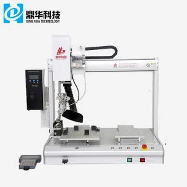
BGA SMD Rework System Hot Air
1.Hot Air and infrared.
2.Brand: Dinghua Technology.
3.Model: DH-A2.
Description
Model: DH-A2
1.Application Of Automatic Optical Alignment BGA SMD Rework System Hot Air
Solder, reball, desoldering different kind of chips: BGA,PGA,POP,BQFP,QFN,SOT223,PLCC,TQFP,TDFN,TSOP,
PBGA,CPGA,LED chip.


2.Advantage of Automated

3.Technical data

4.Structures of Infrared


5.Why BGA SMD Rework System Hot Air is your best choice?


6.Certificate
UL, E-MARK, CCC, FCC, CE ROHS certificates. Meanwhile, to improve and perfect the quality system, Dinghua has passed ISO, GMP,
FCCA, C-TPAT on-site audit certification.

7.Packing & Shipment of CCD Camera BGA SMD Rework System Hot Air

8.Shipment for Split Vision Automatic BGA SMD Rework System Hot Air
DHL/TNT/FEDEX. If you want other shipping term, please tell us. We will support you.
9. Contact us for an instant reply and the best price.
Email: john@dh-kc.com
MOB/WhatsApp/Wechat: +86 15768114827
Click the link to add my WhatsApp:
https://api.whatsapp.com/send?phone=8615768114827
10. Related knowledge of Automatic BGA SMD Rework System Hot Air
How to Make a Chip:
Pure silicon is made into a silicon ingot, which serves as the material for manufacturing integrated circuits in a quartz semiconductor. The silicon ingot is sliced into wafers, which are required for chip fabrication.
Wafer Coating:
A coating is applied to the wafer that is resistant to oxidation and high temperatures. This material is a type of photoresist.
Wafer Lithography, Development, and Etching:
This process involves using chemicals that are sensitive to ultraviolet (UV) light. When exposed to UV light, the photoresist softens. By controlling the position of the mask (or shade), the desired shape of the chip is obtained. The wafer is coated with a photoresist, which dissolves when exposed to UV light. The first mask is applied so that the area exposed to direct UV light dissolves and is then washed away with a solvent. What remains corresponds to the shape of the mask, and this forms the silicon dioxide layer that we need.
Adding Impurities:
Ions are implanted into the wafer to create corresponding P-type and N-type semiconductors. The exposed areas on the silicon wafer are placed in a chemical ion mixture, which changes the conductivity of the doped regions, allowing each transistor to turn on, off, or carry data. A simple chip may use only one layer, but more complex chips usually require multiple layers. This process is repeated, and different layers are connected by creating windows, similar to how PCB boards are made. More complex chips may require multiple layers of silicon dioxide, achieved by repeated photolithography and the above processes to form a three-dimensional structure.
Wafer Testing:
After these processes, the wafer forms a grid of dies. Each die is electrically characterized using a pin test. Generally, there are a large number of dies on each wafer. Organizing the testing process is complex, and mass production of identical-sized chips is crucial to reduce costs. The larger the production quantity, the lower the cost per chip, which is why mainstream chips are relatively low-cost.
Packaging:
The wafers are fixed and bonded, and the pins are fabricated into various package types according to requirements. This is why the same chip core can have different package forms, such as DIP, QFP, PLCC, or QFN. The packaging type is determined by factors such as user application, environment, and market demands.
Testing and Final Packaging:
After the chip has been produced, the final steps involve testing to remove defective products and then packaging the chips.
- Related products:
- Hot air reflow soldering machine
- Motherboard repairing machine
- SMD micro components solution
- LED SMT rework soldering machine
- IC replacement machine
- BGA chip reballing machine
- BGA reball
- Soldering desoldering equipment
- IC chip removal machine
- BGA rework machine
- Hot air solder machine
- SMD rework station
- IC remover device