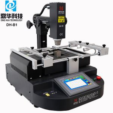
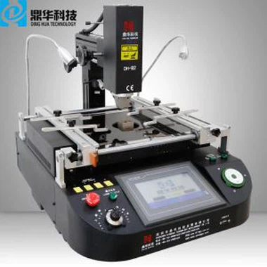
Hot Air Rework BGA Reballing Kit
1. We can offer free training to show How BGA machine works.
2. Lifetime technical support can be offered.
3. Professional training CD and manual come with the machine.
4. Welcome to visit our factory to test our machine
Description
An Automatic Hot Air Rework BGA Reballing Kit is a machine used for removing and replacing Ball Grid Array (BGA)
components on a printed circuit board (PCB). The machine uses hot air to melt the solder joints, allowing the BGA component
to be removed safely.

The reballing process involves picking up a new chip to the BGA component and then reflowing them in place
on the PCB. This is a crucial step in ensuring the reliability of the component after rework.

1. Application Of Automatic
Work with all kinds of motherboards or PCBA.
Solder, reball, and desoldering different kinds of chips: BGA, PGA,POP, BQFP,QFN, SOT223,PLCC, TQFP,TDFN,
TSOP, PBGA,
CPGA, LED chip.
2. Product Features of Automatic
The automatic hot air rework BGA reballing kit is designed to increase efficiency and accuracy in the rework process.
It is a must-have tool for electronics repair and maintenance professionals working with BGA components.

DH-G620 is totally same as DH-A2, automatically desoldering, pick-up, puting back and soldering for a chip, with optical alignment for mounting,no matter whether you have experience or not, you can master it in one hour.

3.Specification of Automatic
| Power | 5300w |
| Top heater | Hot air 1200w |
| Bottom heater | Hot air 1200W. Infrared 2700w |
| Power supply | AC220V±10% 50/60Hz |
| Dimension | L530*W670*H790 mm |
| Positioning | V-groove PCB support, and with external universal fixture |
| Temperature control | Ktype thermocouple,closed loop control,independent heating |
| Temperature accuracy | +2℃ |
| PCB size | Max 450*490 mm, Min 22 *22 mm |
| Workbench fine-tuning | ±15mm forward/backward,±15mm right/left |
| BGA chip | 80*80-1*1mm |
| Minimum chip spacing | 0.15mm |
| Temp Sensor | 1(optional) |
| Net weight | 70kg |
4.Why Choose Our Automatic Hot Air Rework BGA Reballing Kit?


5. Certificate of Automatic
UL, E-MARK, CCC, FCC, CE ROHS certificates. Meanwhile, to improve and perfect the quality system, Dinghua
has passed ISO, GMP, FCCA, and C-TPAT on-site audit certification.

6. Packing & Shipment of Automatic

7. Shipment for Automatic
DHL/TNT/FEDEX. If you want another shipping term, please tell us. We will support you.
8. Terms of Payment
Bank transfer, Western Union, Credit Card.
Please tell us if you need other support.
9. Related Knowledge
Cause Analysis and Prevention of PCBA Assembly Explosion – Analysis of Causes of Explosion
1. What is an explosion?
An explosion is the common term for delamination or foaming of printed circuit boards (PCBs).
- Delamination refers to the separation of layers within the substrate, between the substrate and the conductive copper foil, or within any other layer of the PCB.
- Foaming is a type of delamination that manifests as local expansion and separation between any layers of the laminate substrate or between the substrate and a conductive copper foil or protective coating. Foaming is also considered a form of stratification.
2. Analysis of the Causes of Explosion
The customer's products are used in industrial-controlled inverters. The design requirements specify PCBs with CTI (Comparative Tracking Index) values. This 4-layer PCB has special requirements in the production and application process. Due to the special nature of the CTI > 600 copper-clad material, it cannot be directly pressed with the inner layers. This type of material must be pressed with different types of interlayer insulating prepreg materials to meet CTI standards and lamination bonding force requirements.
Due to the use of two kinds of prepreg insulation materials, the two materials have different resin types. The bonding strength of the fusion interface between these two insulation materials is relatively weak compared to the single insulation material used in conventional 4-layer boards. When the PCB absorbs moisture to a certain extent in its natural state, and then undergoes wave soldering or manual plug-in soldering, the temperature rises from normal room temperature to over 240°C. The moisture absorbed in the board is then instantaneously heated and vaporized, generating internal pressure. If the pressure exceeds the bonding strength of the insulating layer, delamination or foaming occurs.
In general, explosions are caused by inherent deficiencies in the materials or the process. These deficiencies include:
- Materials: The copper-clad laminate or the PCB itself.
- Processes: The production process of the copper-clad laminate and the PCB, the PCB production process, and the PCBA (Printed Circuit Board Assembly) assembly process.
(1) Moisture Absorption During PCB Manufacturing
The raw materials used in PCB manufacturing have a strong affinity for water and are easily affected by moisture. The presence of water in the PCB, the diffusion of water vapor, and the change in water vapor pressure with temperature are the primary causes of PCB explosions.
The moisture in the PCB mainly exists in the resin molecules and physical structural defects inside the PCB. The water absorption rate and the equilibrium water absorption of epoxy resin are determined by the free volume and the concentration of polar groups. The larger the free volume, the faster the initial water absorption rate, and the more polar groups there are, the higher the moisture absorption capacity. As the PCB is reflow soldered or wave soldered, the temperature increases, causing the water molecules and the water in hydrogen bonds to obtain sufficient energy to diffuse in the resin. The water then spreads outward and accumulates at physical structural defects, causing an increase in molar volume. Additionally, as the welding temperature increases, the saturated vapor pressure of the water also increases.
According to data, as temperature rises, the saturated vapor pressure increases sharply, reaching 400 P/kPa at 250°C. If the adhesion between the layers of material is weaker than the saturated vapor pressure generated by the water vapor, the material will delaminate or foam. Therefore, moisture absorption before soldering is a significant cause of PCB explosions.
(2) Moisture Absorption During PCB Storage
PCBs with CTI > 600 should be treated as moisture-sensitive devices. The presence of moisture in the PCB significantly impacts its assembly and performance. If a PCB with a high CTI value is stored improperly or exposed to moisture, it will absorb water over time. Under static conditions, the water content of the PCB will gradually increase. The difference in water absorption rates between vacuum-packed PCBs and those without proper storage is illustrated in the figure below.
(3) Long-Term Moisture Absorption During PCBA Production
During the production process, prolonged exposure to moisture or other factors can lead to moisture absorption in PCBs with CTI > 600. If the PCB undergoes soldering after absorbing moisture, there is a risk of delamination or foaming.
(4) Poor Soldering Process in PCBA Lead-Free Production
For lead-free soldering in PCBA production, Sn53/Pb87 solder has been replaced by SnAg-Cu lead-free solder, which has a higher melting point (217°C vs. 183°C). As a result, reflow soldering and wave soldering temperatures have increased from 230-235°C to 250-255°C, with the peak temperature possibly being even higher. During the soldering process, if the soldering time is too long or if the temperature rises too rapidly, the PCB may suffer from poor production quality, which increases the risk of delamination or foaming.